Using The Xilinx Foundation Series Software:
Schematic Entry
- In the Win95 Start Menu select
Programs, then select the program group
Xilinx FoundationSeries. In this group
click on Xilinx Foundation Project Manager.
- Select New Project in the File menu. Type in the project name that you
will be working on, ex. "4bitPrm". The correct settings for Type,
Family, Part, and Speed must be set to the values shown below. This is
important.
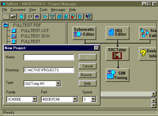
- Click OK. The
Project Manager window should appear.
The Project Manager window will be
used to coordinate all aspects of the design process.
- Click on the Schematic Editor box
 in the Project Manager. The Schematic Editor window should appear with
a blank schematic.
in the Project Manager. The Schematic Editor window should appear with
a blank schematic.
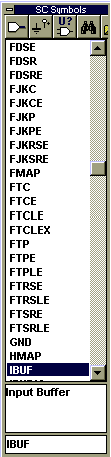
- To add parts to the schematic, you will need the SC Symbols Toolbox. Select
 or use the quick key F3. The SC Symbols Toolbox should appear.
Note: The cursor can take on several different functions
in the Schematic Editor window. The cross-hair is the general cursor, and it is
used to select buttons in the Schematic
editor window, select and move parts in the schematic,
and to select parts for placement in the SC Symbols toolbox.
The AND gate cursor is utilized when a part is selected from the
SC Symbols toolbox to be placed in the schematic. The Pen cursor
is utilized when wires are being drawn. The AND gate and Pen
cursors can be switched to the cross-hair cursor by selecting the
button that is an Arrow in the Schematic
Editor window.
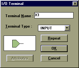
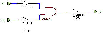
- Because this schematic will be directly programmed into the FPGA, all
inputs and outputs must have buffers and pads attached. For inputs, the
first part is the I/O pads. Select the I/O terminal
button
 and the I/O Terminal
window will appear.
and the I/O Terminal
window will appear.
- Give the terminal a name, and chose its function, input or output,
click OK, then place it in the design.
- Buffers must be placed between the logic circuit and its inputs and
outputs. The IBUF (Input Buffer) must be selected from the SC Symbols toolbox and placed after each input.
The OBUF (Output Buffer) must be selected and placed before each
output. Leave ample space between parts to allow for wires, but do not
place wires yet.
Note: When placing multiple parts of the same type, you do
not have to select it in the SC
Symbols window each time, if the cursor looks
like an AND gate then you can click on the part in the schematic
that you would like to place again, and an exact copy of that part will
be available through the cursor to be placed again.
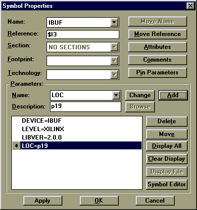
- The pin number on the FPGA has to be specified in each of the IBUF
and OBUF parts. Change the cursor mode into the cross-hair, and then double
click on the IBUF or OBUF whose pin you would like to set. A Symbol
Properties window will appear. In the Parameters section
of this window you must add a parameter by selecting LOC
in the Name box. Then in the Description box the pin number must be assigned,
ex. P19. Select the Add button,
and the list of parameters should now have LOC=p19. Click on Apply and then click on OK to return to the updated schematic.
- Select and place the rest of the symbols in your design. Note:
You can search for the symbol you want by typing part of its name in the
Symbol
window, and then a short description of the part
should appear.
- Wires must now be placed to connect all of the gates, inputs, outputs,
and buffers. Select the Draw Wires
button
 in the Schematic Editor window
toolbar, or use the quick key F4. Click
on one of the lines extending from the gates and then click on the other
gate, OBUF, or IBUF to connect those parts together. Wire all of the parts
in this manner.
in the Schematic Editor window
toolbar, or use the quick key F4. Click
on one of the lines extending from the gates and then click on the other
gate, OBUF, or IBUF to connect those parts together. Wire all of the parts
in this manner.
- To perform an integrity test, pull-down the Options
menu and select Integrity Test, or
use the quick key Ctrl-F2. To create
a netlist pull-down the Options menu
and select Create Netlist, or use the
quick key Shift-F2. The design should
now be ready to simulate.
See: Using
Xilinx Foundation Series Software: Function Simulation In the Waveform Viewer
Download a Microsoft Word 95 7.0 printable text only version of this document:
SchematicEntry.doc
Back to Xilinx Foundation Series Main Menu